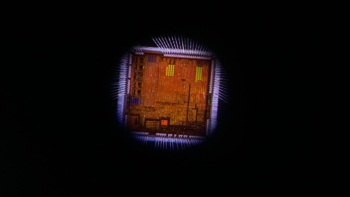
The European Commission has given the go-ahead for Austria to provide €319 million in state aid to Infineon Technologies, supporting a €1.1 billion overhaul of its semiconductor plant in Villach, Carinthia. The project aims to turn the facility into the world's first high-volume manufacturing site for next-generation gallium nitride (GaN) power semiconductors on 300-millimetre wafers.
The approval, announced on 28 October, falls under the EU Chips Act, a framework designed to bolster Europe's semiconductor industry and reduce dependence on imports from Asia and the United States. The Commission stated that the measure will “strengthen the EU's position and autonomy in the semiconductor value chain.”
The bloc has set an ambitious target of doubling its global market share in semiconductor production from 10% in 2023 to 20% by 2030. The Chips Act also aims to stimulate demand for European-made chips and help domestic suppliers scale up.
A strategic investment for Europe
Infineon, a German company headquartered in Neubiberg near Munich, says the investment will establish its Villach site as a “global competence centre for power semiconductors.” The company already holds a 29% share of the global power semiconductor market and a 50% share in automotive chips.
Austrian Chancellor Christian Stocker called the project “one of the largest single investments in the history of Austria's high-tech industry.” He added: “This is not only a strong commitment to Austria as a business location but also helps ensure that the future of the semiconductor industry will not be shaped solely in Asia or the United States, but also in Austria and Europe.”
Infineon's CEO, Jochen Hanebeck, emphasised the company's commitment to European technological sovereignty. “This substantial investment shows our clear commitment to strengthening the European semiconductor ecosystem and Europe's technological sovereignty,” he said. “By establishing high-volume manufacturing on 300-millimetre wafers, we will be the first company in the world to bring gallium nitride power electronics into volume production.”
Why gallium nitride matters
Gallium nitride is increasingly replacing silicon in power electronics because it can handle higher voltages, switch faster, and tolerate higher temperatures. These properties make GaN semiconductors ideal for a wide range of applications, from smartphone chargers and laptops to AI data centres, electric vehicles, solar panels, wind turbines, 5G and 6G base stations, and robotics. Their energy efficiency is particularly valuable in reducing power consumption.
The move to 300-millimetre wafers—larger than the conventional 200-millimetre versions—allows 2.3 times more chips to be produced per wafer, significantly lowering manufacturing costs. Infineon says it was the first company to successfully process 300-millimetre GaN wafers in 2024.
Analysts project the GaN power semiconductor market will reach approximately $3.1 billion by 2031, with annual growth of around 35% between 2025 and 2031. This growth is driven by the accelerating adoption of electric vehicles, renewable energy systems, and AI infrastructure across Europe and globally.
The approval comes as the EU continues to push for greater self-sufficiency in critical technologies. The EU's startup plans have faced hurdles, but this investment signals a concrete step forward in the semiconductor sector. The Commission's decision also aligns with broader efforts to enforce digital regulations and ensure that European companies can compete on the global stage.
For Austria, the project is a major boost to its high-tech industry and its position as a business location. For Europe, it represents a tangible move towards the goal of doubling its share of global chip production by 2030.